Needing more than a spark test?

XRF used to sort "clean" aluminium - apparently.
I came across a video about recycling aluminium, and I admit I did not get way into the detail, but I am sure this is a direct application of XRF.

We see a (huge) set of 160 keV sources used to blast X-rays onto cut up chips of recycled aluminium on a special conveyor which uses specially controlled air blasts to knock the detected alloys into their sorting receptacles. Given the low, almost transparent nature of aluminium to X-Rays, I guess the machine might be detecting the contaminating alloy elements instead. Of course, it's way out of my league, but interesting.
The first 4 minutes relates to XRF

The most impressive thing to me is fact that the machine is doing it so fast! BTW, I think your hypothesis is correct. The 160Kev's may be to excite some of the inner shell electrons to get more distinct x-ray lines. Maybe :dunno:

It also is interesting that, despite the high tech approach, they still have someone next to the conveyor belt to pluck the odd bits out.

On a slightly different subject, although it hasn't rained for about 3 weeks now, it's supposed to get into the 90's the next three days. Some inside activity to escape the heat may actually include working on my HV PSU.
 
The most impressive thing to me is fact that the machine is doing it so fast! BTW, I think your hypothesis is correct. The 160Kev's may be to excite some of the inner shell electrons to get more distinct x-ray lines.
If that's the exciting voltage, it'll make significant over-10keV photons, and copper K shell fluorescence
would show up. Copper (old duraluminum, and 2000 series alloys) is OK for structures, but not
for corrosion resistance, and you'd want to segregate accordingly.
 
@graham-xrf
I know you were interested in trying to directly work with the RPI kernel and avoid a microcontroller. I was looking into linuxcnc which gets used on RPI's often, I'll pass on some hints from there: "cpusets" and "isolcpus" are two linux keywords you might want to investigate. Both are mechanisms to lock out a cpu core from normal timesharing and limit them to tasks. isolcpus is a grub/kernel boot flag, cpusets is a more general runtime concept. Lots of details tangled up in all that, I won't pretend to know more than passing on suggestions.
 
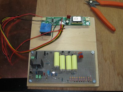
I have a couple of updates regarding this project. The first is that I decided to put my prototype PMT power supply on a breadboard. Mostly just to clean it up and make it a bit more robust while I play with the PMT. And by breadboard I MEAN breadboard :)

IMG_2124.JPG

The square block between the CCFL inverter and my hand-wired controller board is a home-made inductor, designed to isolate the controller board from the inverter. Not shown is my opto-isolator circuit which will replace the inductor and permit the use of a separate 12V supply to run the noisy inverter. Of course, I will need to connect the inverter's ground line to the controller because I need a feedback path to set the output voltage. Since it will be a single-point ground it should be OK in terms of minimizing noise from the inverter.

The heat-sunk power transistor on the controller board originally supplied the variable-voltage drive to the inverter but in my new approach it will drive my opto-isolator's LED input side. The power transistor and heat sink will be overkill but I don't feel the need to replace it with this version of the controller.

The second update is to report that I just ordered a 4x4mm SiPM to play with. It has a BGA footprint so will require a custom PCB. Not to mention a scintillator crystal, but I already have a LYSO crystal. Not the best for energy resolution but at least it's not hygroscopic!
 
I have a couple of updates regarding this project. The first is that I decided to put my prototype PMT power supply on a breadboard. Mostly just to clean it up and make it a bit more robust while I play with the PMT. And by breadboard I MEAN breadboard :)

View attachment 457239

The square block between the CCFL inverter and my hand-wired controller board is a home-made inductor, designed to isolate the controller board from the inverter. Not shown is my opto-isolator circuit which will replace the inductor and permit the use of a separate 12V supply to run the noisy inverter. Of course, I will need to connect the inverter's ground line to the controller because I need a feedback path to set the output voltage. Since it will be a single-point ground it should be OK in terms of minimizing noise from the inverter.

The heat-sunk power transistor on the controller board originally supplied the variable-voltage drive to the inverter but in my new approach it will drive my opto-isolator's LED input side. The power transistor and heat sink will be overkill but I don't feel the need to replace it with this version of the controller.

The second update is to report that I just ordered a 4x4mm SiPM to play with. It has a BGA footprint so will require a custom PCB. Not to mention a scintillator crystal, but I already have a LYSO crystal. Not the best for energy resolution but at least it's not hygroscopic!
One way to further reduce noise coming from the inverter would be to separate the inverter transformer's secondary winding from the inverter board's ground. However, so far my examination of the inverter board has not revealed a way to do this. I bought two CCFL inverter boards so one way to get to the bottom of that would be to de-solder the transformer on the "spare" to see how it's connected up. Ohming out the HV outputs to likely points on the circuit board was a fruitless endeavor so a more invasive approach appears to be needed. I used to have access to a high-resolution x-ray machine, which I used on occasion to reverse-engineer circuit boards and I miss it now!
 
One way to further reduce noise coming from the inverter would be to separate the inverter transformer's secondary winding from the inverter board's ground. However, so far my examination of the inverter board has not revealed a way to do this. I bought two CCFL inverter boards so one way to get to the bottom of that would be to de-solder the transformer on the "spare" to see how it's connected up. Ohming out the HV outputs to likely points on the circuit board was a fruitless endeavor so a more invasive approach appears to be needed. I used to have access to a high-resolution x-ray machine, which I used on occasion to reverse-engineer circuit boards and I miss it now!
I have figured out which pins are the secondary side of the inverter so isolating it from the CCFL drive electronics may be possible. It remains to be seen if the inverter's fault protection will kick in if I do that. So that will be a last resort. I also discovered that the "HV" and "LV" labels on the inverter's output connectors actually are reversed. I couldn't get the output any higher than about 700V until I reversed the HV connections to my regulator board. Now I can get over 1KV. Sweet!

I have gotten the opto-isolator circuit wired in and working, but still am seeing a fair amount of noise on the HV output. I'm pretty sure it's the HV pulses coupling into the output because doing a bit of haphazard shielding greatly reduced the noise. As a result, I have gone on a bit of a tangent -- learning how to use my cheap Harbor Freight metal brake to make small boxes. Sheet steel would be much better in terms of magnetic interference but for starters I'm going with aluminum. Mostly because I already have some sheet aluminum that's the right thickness.

Pre-made boxes are, in my opinion, outrageously over-priced. So learning how to make my own has been on the to-do list for awhile.
 
Pre-made boxes are, in my opinion, outrageously over-priced.
I agree. I think it has to do with the cost of getting UL approval.
I've made some using aluminum. My 3 in one brake didn't like the thickness of the aluminum I had on hand. So I put it on the mill and cut some shallow V-grooves where the bends go. Grooves are on the inside so the bends look nice and square-ish on the outside.
 
This post is mostly for @graham-xrf. I recently found some decent looking matched JFET pairs for a relatively decent price that may be worth looking at for a low noise, high speed TIA. They are the JFE150 and JFE2140. The latter is slightly better with regard to Cin @13pf. Both P/N's have very good Gm and noise levels in the 1nv/sqrt-hz range. Digikey USA has them in stock. They are part of the IP that Texas Instruments got when they bought Burr-Brown.
 
This post is mostly for @graham-xrf. I recently found some decent looking matched JFET pairs for a relatively decent price that may be worth looking at for a low noise, high speed TIA. They are the JFE150 and JFE2140. The latter is slightly better with regard to Cin @13pf. Both P/N's have very good Gm and noise levels in the 1nv/sqrt-hz range. Digikey USA has them in stock. They are part of the IP that Texas Instruments got when they bought Burr-Brown.
Thank you for thinking of me. I have hopes of getting back into my favourite hobby, but for the present, I have to deal with a debilitating condition, in addition to my wife requiring more surgery next week. Regrettably, I can no longer even fly sailplane gliders, sharing thermals with birds of prey over (UK) Hampshire. To do such stuff, one has to at least be able to climb in!

I take inspiration from you all, folk like @rabler, who has been very kind despite having worse problems than I have. For now, I shall stay with this community, and contribute when I can.
----
When it comes to very low noise front-end high gain stuff, JFE150 and JFE2140 with the low shot noise could indeed be useful, say in the role of the front-end JFET in that extreme performance TIA we have already modeled. I have noticed that many JFETs from the 1990s, often used for high class audio pre-amps, just fit right in when used as part of TIAs working with modern op-amps. Some are simply the same old FET designs, re-named and outrageously priced, offered at the audio fans (eg. those LSK170 and similar from Linear Systems).

By every considered calculation, there seems a reasonable chance that one can achieve low noise gains greater than 1e+05 to compete with photomultipliers. The key property in comparing the two approaches is right up at the sensor. It is about how good are high area PIN diodes vs scintillator crystals feeding PMT photocathodes made of exotic materials.
Graham,
I'm very sorry to hear about you and your wife's difficulties. I had noticed that you weren't posting much of late and had wondered if something was amiss. I wish a speedy recovery for both of you.
 
Back
Top