Needing more than a spark test?

Logic ICs ?
Yes - this happens when you need to scatter some glue logic between the computing stuff and measurement bits.
In the lower left corner of the A/D circuit of AD7622, there is a D-Type Latch which lets in the low jitter clock.
There is a "Note 7", which did not help much.
It's been a very long time since I used something like 1/8 of a 74273.
3.3V has arrived (and almost moved on!)

So what is the modern choice? Maybe MC74AC273 costing £0.94, or something with a "T" in the part number?
Its a 20-pin SOIC. That's enough space to fit two whole A/D converters!
One wonders what the remaining 7 of those D-Latches might be useful for. :)
You might be able to find some single gate stuff in small packages. Makes a whole lot more room for other stuff!
 
You might be able to find some single gate stuff in small packages. Makes a whole lot more room for other stuff!
It seems there ARE such things.
Duh! OnSemi NC7SZ373 is one of them They call it "Ultra High Speed". Then we see the rise and fall times not using time units. A slew rate is quoted instead at 10nS/V. Assume 3.3V, and that be 33nS. I do not think that to be "ultra" anything at all!

BUT - since such tiny things do exist, we keep looking - and so find the Ti device SN74LVC1G373 in a 6-pin SOT23, or in a truly tiny 6-Pin SC70
An entire pulse in 3nS is much better, though still not managing to impress me much (after Shania Twain?)
 

Attachments

  • NC7SZ373-D.PDF
    358 KB · Views: 3
  • sn74lvc1g373.pdf
    769.4 KB · Views: 1
Last edited:
I finally got my HV power supply working the way I want. While it had no measurable ripple it took a very long time to settle down. It behaved as a lightly damped oscillator, with a period of about 1 second. And if I imposed a brief load on the output it would again go into its damped oscillation.

This probably was due to a couple of things. My circuit simulations suggested that the loop gain was way too high -- not surprising, since the CCFL inverter can step 12V up to something on the order of 2KV (probably more, with no CCFL lamp loading it down). The other problem was that I've got three low-pass filter stages in there so the combination of lots of phase shift and high loop gain resulted in the poor gain margin. Three filter stages probably is overkill, but the Theremino folks really push the concept of very low HV supply ripple for the PMT.

My solution(s) included a nonlinear clamping circuit that in effect greatly reduces the loop gain once the control voltage to the inverter gets close to the necessary setpoint (determined by measuring it), and adding some lead compensation -- basically, adding some "D" to my PID-like HV controller. The latter was easy enough to do, since I had a high-pass RC filter on the controller board to monitor the output ripple.

With all this the output exhibits no overshoot and no low-frequency ringing. The next step is to modify the voltage divider on my PMT to make it compatible with the Theremino approach to things. This will require that I remove the bottom cap on the PMT/scintillator enclosure. I will follow
this procedure to do it. Hopefully the scintillator survives!
I took the other approach to losing the ripple and SMPSU noise, using much less capacitor and low pass energy storage filtering. The context was not as tricky as your need for 2kV, but much more modest for providing B+ voltage for some vacuum tube circuits. When it comes to easy switch-mode kit, there is a ton of choice, but near zero available at voltages above 48V. Those convenient (and cheap) Chinese SMPSU modules are so handy, but need to be followed by something to take out the ripple. I "regulate it away" by using high bandwidth linear regulators, fast enough to squish even the kHz noise.

To get my 135V (and up to 300V), I use the trick shown by FesZ Electronics YouTube guy, by using a high voltage MOSFET ahead of a LM317-type regulator, such that the MOSFET takes the main task, and delivers a quite smooth pre-regulated input to the final 3-terminal regulator, which never sees any voltages across it exceeding it's ratings. The final regulator operates stood at a voltage high enough so that its main job is to be the noise ripple filter. When I used filter capacitors too large, it was capable of violent high voltage oscillation. I must have made a huge racket all over the HF bands!

You are absolutely right about the phase lags when it comes to heavy low pass filtering. Provided the filtering is entirely passive, that's all OK. Not so if the end result is being used to feed back to anything in control of what starts out. They add up to give you oscillation.

I also use the venerable TL431(s) as low noise artificial zeners, sometimes stacked, to reduce the division fraction of the voltage sampler potential divider. At 2KV, even 1Meg Ohm in the chain would get hot (4W). Getting a clean, low noise reference at some voltage nearer to the one you are trying to clean up is what I was after. The attached picture is what I used to make a 135V supply, with noise and ripple cleaned out, without blowing up the three-terminal regulator. They can only stand about 40V max. Beware, without R7, you make a high power RF oscillator! Also, I added D3 to keep Vgs sane. It did not oscillate in simulation, but it sure did in actual build. Bursts of several hundred kHz, and maybe some MHz, all happening at an audio rate. R7 and D3 have yet to be tried in real build.
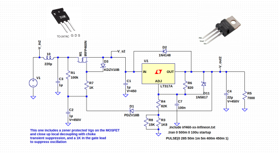
T-175-PSU-2xx.png
PS - Forgive the little images of the MOSFET and regulator. It helps me orient when I am trying to assemble it, and I am looking at the underside, to remember which is the gate, or the ADJ. As is, the circuit is no good for something like 2kV without R4, R8, R3 becoming exceptional, but I use it only for illustration of getting at the ripple without fat filters.
 
Last edited:
Beware, without R7, you make a high power RF oscillator!
I learned about damping resistors on the gate of power MOSFETs when I was experimenting with using them in audio power amplifiers. It was "magic" to go from otherwise untameable oscillations to well-behaved operation.
 
If you are only doing low currents, a circuit board mounted choke can be a tool to notch up your filtering without a lot of resistive losses. That simplifies the high voltage insulation issues with a chassis mount high current unit.

Sent from my SM-S911U using Tapatalk
 
This is an update regarding the PMT/Scintillator voltage-divider modifications. I was able to remove the aluminum plug, exposing the voltage divider. The circuit board is exactly the same design that's shown in the link I posted above. The detector I got is different because it has some wires coming out the other end. I haven't found anything on the web describing what they might be for. There is a high resistance between two of the wires but.....I'm not sure what that means. If it is something meant to monitor the health of the NaI detector, leakage through the crystal would likely signify that the scintillator has absorbed water (a Bad Thing). Fingers crossed there!
 
@homebrewed Mark - can scintillator crystals ever be "dried out" or recovered in any way? Here I am thinking how we restore silica gel dessicant crystals by baking them, or using a vacuum pump? I am guessing that if there was a good way to make a scintillator good again, most folk possessing one would have done it long ago.
 
@homebrewed Mark - can scintillator crystals ever be "dried out" or recovered in any way? Here I am thinking how we restore silica gel dessicant crystals by baking them, or using a vacuum pump? I am guessing that if there was a good way to make a scintillator good again, most folk possessing one would have done it long ago.
I have read some accounts where someone with a "wet" crystal baked it in an attempt to restore it. It apparently caused a partial recovery, because the typical reddish color of a damaged crystal did lighten up -- but didn't become water-white. The problem could be that NaI crystals are easily cracked by thermal stress, and cracks will definitely trash the energy resolution. So pulling a good vacuum on one, instead of heating it, might work better.
 
Back to my concern regarding those extra wires, I found a document published by Scionix that suggested they probably are some kind of calibration system -- an LED and a photodiode. It would be nifty if that could be used in some way to further improve the energy resolution of the PMT/scintillator, but, lacking any real details, it would be difficult to take advantage of it. There also is the fact that their calibration system -- if that's what it is -- appears to be unique. If there was some significant resolution improvement I'd think that most everyone would be using it.
 
Back
Top